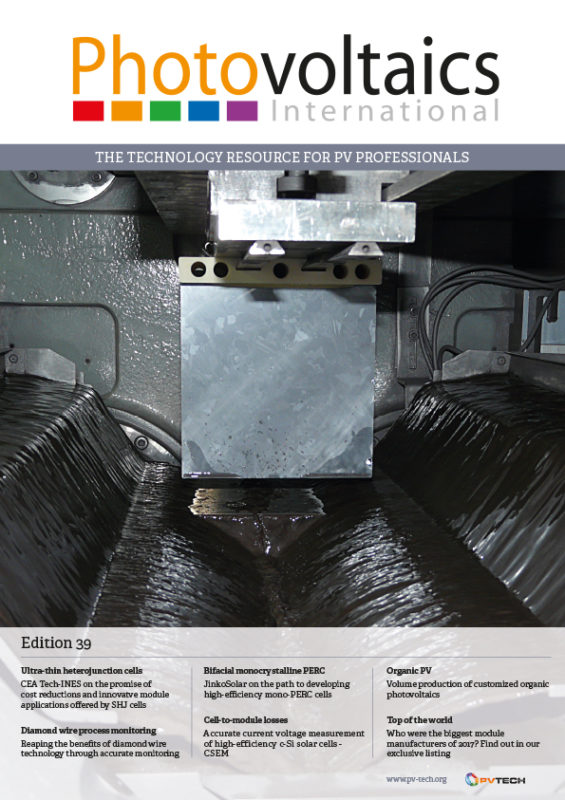
Welcome to the thirty-ninth edition of Photovoltaics International. We go to press just a few days after the conclusion of our PV CellTech conference in Penang. The focus for all the PV CTOs, chief scientists, materials providers, equipment manufacturers and others gathered for the summit was how to keep pushing the industry towards a standard 20% efficiency while also expanding in scale. That expansion ought to be 100GW in three years if demand is to be met, according to one speaker.
CEA-INES researchers look at the benefits of exploiting the symmetrical a-Si/c-Si/a- Si structure of silicon heterojunction cells to use ultrathin wafers.
Another innovation that delivers materials savings is of course diamond wire sawing and, again, scale and efficiency are dual drivers. Here, CEA demonstrates the need for, and processes involved in, closely monitoring the cutting process to ensure wafer quality is consistent and productivity can remain at the desired level.
We look at different sides of bifacial technology (pun intended) starting with JinkoSolar’s appraisal of its mono PERC bifacial cells built using standard production technology and racking up average efficiencies of 21.8%.
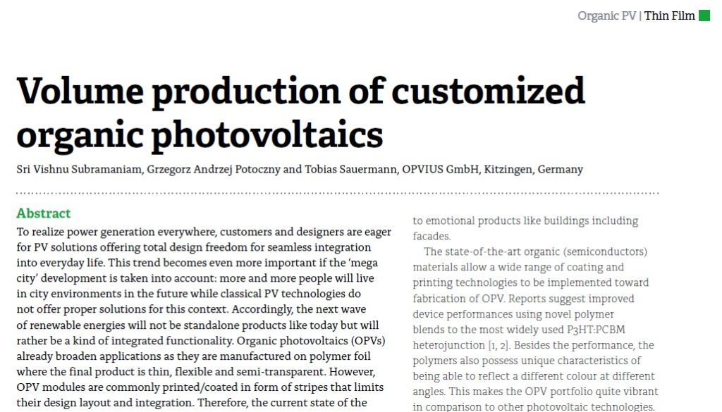
Away from the crystalline silicon world, German research firm OPVIUS explores how a combination of printing methods could open the door to freeform PV modules, unleashing an entirely new suite of product options and applications.
ECN Solar reveals the results of an industrial-scale trial process to develop an n-type bifacial IBC solar cell that is based on tube diffusion and a simultaneous single-step screen-print of contacts at both polarities.
Last but not least, CSEM looks at the impact the emerging diversity in cell technology and module architecture is having on metrology.


