By Kyung Nam Kim, Green School, Korea University, Seoul; Yoonmook Kang, Green School, Korea University, Seoul; Jeong Min Lee, Wonik IPS, Gyeonggi-Do, South Korea; Dong Seop Kim, Wonik IPS, Gyeonggi-Do, South Korea
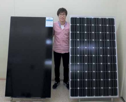
Of the various copper indium gallium diselenide (CIGS)-formation processes, a so-called ‘two-stage process’, consisting of sputtering and selenization, has been successfully applied in large-scale production thanks to its stable process scheme and high-fidelity production equipment. A CIGS module with a power of 231W, corresponding to a total area-based efficiency of 16% for 902mm × 1,602mm, was demonstrated when this twostage process was employed in a pilot production line at Samsung (although all the technology concerning CIGS production has now been transferred to Wonik IPS, whose main business is to provide production equipment for the semiconductor and display industry). The high-power module suggests significant potential for CIGS modules to compete with multicrystalline Si modules in terms of both cost and performance. This paper addresses the
important process technologies for achieving high efficiency on large-area substrates, and presents a cost analysis using the data obtained from the operation of the pilot production line. As a result of the synergistic effect of low material cost and high efficiency of the two-stage process, the CIGS manufacturing cost is expected to be reduced to US$0.34/W.


